xPDK_BB
This section in a xPDK extends from xPDK_Header.This BB information contains the typical shared data between software:
- building blocks
- their parameters
- connections
- user interface behavior
- simple layout information
- references to compact model information
This scope is therefore fairly broad and future extensions are likely to capture more information. The current common fields provide for a rich design kit already compared to other formats, while adressing different software.
Vendor extensions are supported in this section, so software specific details are possible therefore to tune behavior.
Extensive example
This example is part of the full file below. It is mostly listed here so you do not need to download it. It shows many fields and properties that can be defined and these are described in the child pages.This file includes the technology file and adds the Met, Met1 and Met2 xsection's in the meta data to show both options work.
Use:
xmllint - -format - -xinclude - -schema xPDK_BB.xsd xPDK_BB.xmlStructure
The attributes and elements are shown below, in a sorted per type fashion.In case a list is printed after an element, it indicates that you can have many, otherwise it should be a single element. With a optional it tells the element is not required.
<xPDK_BB dmCategoryAsList="..." dmHide_bbstyles="..." dmHide_bbtypes="..." generateDRC="..." generateDerived="..." generateLVS="..." pdk_name="..." pictsize="..." portMapDC="..." portMapDCi="..." portMapDCo="..." portMapIn="..." portMapOut="..." portMapRF="..." portMapRFi="..." portMapRFo="..." ... > ...
<bb> ... </bb> list
<bbAnnotateFontSize> ... </bbAnnotateFontSize> list
<bbAnnotateName> ... </bbAnnotateName> list
<changelog> ... </changelog> list
<feature> ... </feature> list
<group> ... </group> list
<parameter_accuracy> ... </parameter_accuracy> list
<run_name> ... </run_name> list
<software> ... </software> list
<ticket> ... </ticket> list
<xPDK_CompactModel_List> ... </xPDK_CompactModel_List> list
<xPDK_Layout> ... </xPDK_Layout> list
<xsection> ... </xsection> list
<xPDK_Header:MRL> ... </MRL> optional
<xPDK_Header:TRL> ... </TRL> optional
<xPDK_Header:attribute> ... </attribute> list
<xPDK_Header:doc> ... </doc> list
<xPDK_Header:global> ... </global> list
<xPDK_Header:groupRef> ... </groupRef> list
<xPDK_Header:license> ... </license> optional
<xPDK_Header:provider> ... </provider> optional
<xPDK_Header:tapeout> ... </tapeout> list
<xPDK_Header:tex> ... </tex> list
<xPDK_Header:version> ... </version> list
</xPDK_BB>
XSD The schema file can be downloaded or viewed at xPDK_BB.
Details
Type xPDK_Header
Most is optional and extension capability is the idea.
bb
Define a series of building blocks, sometimes called cell or pcell also (EDA terminology).This section is used by both layout and schematic / circuit oriented software to allow designers to create their circuits. In general it does not make sense to have design kits without BBs in there. However it is not a required to have them - there are gds layer / process only design kits also.
It is possible to use global variables defined in layout.xml in the expressions here, for example to set default waveguide widths. For example:
layout.xml:
bb.xml:
Type pdaBBdefinition documentation: BB definitions including ports, parameters, attributes and views.
Basic fields
The following example shows the basic information that is expected (but not required). With this content you can start using it in different software. It does not define parameters, so it is a fixed design.Normally BB's have more
ports as well as parameters, so a "real" BB will be longer.
Documentation
Adding documentation is easy also, thedoc is used by more software then the
tex. tex is for long pieces of text like full help pages.
Alignment
A building block can be validated on angle - this is using the "org" port as coordinate reference.You can select one of the following options: Manhattan, Xaligned, Yaligned, Angles as a series of values
Note that the global position of this is relevant; if you use the BB in your library and thus create a design hierarchy, the (relative) location inside the library netlist/component is not relevant.
Check definition
The xPDK format allows many aspects to be defined. To check that you defined it correctly, you can use the xsl files that convert the definition to the software of your choice.A basic option is to use the gdspy project. The xsl/xPDK_toPython.xsl can use this library to generate the basic curves / black box designs. You can convert the BB.xml (as that includes the Layout.xml) in a simple script to generate a pdk.py.
xmllint --xinclude BB.xml | xmlstarlet tr $XPDK/xsl/xPDK_toPython.xsl -s pdkiteration=0 -s whitebox='nocell' > export/pdk.py
This (large) python file uses the xPDK Geometry.py and gdspy code jointly to allow the different boundary views, port locations and so on to be written to a GDS file or shown on screen.
Suppose you want to test the definition of a BB called myBB that has a paramter Length. Create a test.py with the following content:
from Geometry import Design
from pdk import *
myDesign=Design('/tmp/myBB.gds')
t=myBB()
t.Length=10
e0=t.place(myDesign,"element0",org=[0])
#e0.print_boundary()
t.Length=20
e1=t.place(dp,bir=e0.bol)
#e1.print_boundary()
#myDesign.draw_gdspy() # Just generate GDS
myDesign.draw_gdspy(show=True) # Show on screen
myDesign.write()
This should place two myBB's on the design, one with Length=10 and one with Length=20. The GDS file will depend on the type of BB (whitebox or not) and the -s whitebox='nocell' command line option. For black-box and grey-box BBs you should see two GDS cells, one per parameter setting.
bbAnnotateFontSize
Type bbAnnotateFontSize documentation:bbAnnotateName
Type bbAnnotateName documentation:changelog
Type xPDK_ChangeLog documentation: list, which can be empty. Software or design kit providers are not required to fill this data when changes are made, but it can help users to see what changed over time.dmCategoryAsList
Type epibool documentation: Wrap a boolean for name space API aspects.dmHide_bbstyles
Type epibool documentation: Wrap a boolean for name space API aspects.dmHide_bbtypes
Type epibool documentation: Wrap a boolean for name space API aspects.extend
Type AllowExtend documentation: Allows to extend with any (complex) data for enriching a design kit. The sub-data of an
extend will normally be vendor or provider specific, but may span multiple software
vendors or suppliers.Provider extensions can be references to (or embedded) reporting scripts or their versions; source database references and so on. Such data is helpful in cross-referencing production issues or differences between export snapshots. Embedding such data in the XML rather then side-files enhances tracebility and reduces errors.
Using this section is not considered part of the xPDK format therefore, but as long as the files validate with the Stichting PDAFlow Foundation schema's, it is not considered a (not allowed) Derivative version.
For conventions, please check also Extensions.
See also xPDK License.
feature
Type feature documentation: Define the features that are availble for use with this PDK in the given software.This information is used in the design manual creation but can be embedded in the software specific design kit also.
- layer Provide the layer / color maps for display so you can load gds files from other software easily also.
- layout Defines a `layout-only' scope design kit, suitable for basic chip design.
- autorouter List the xsection/mcs's for which auto-routing are enabled.
- basic-connector
List the xsection/mcs's for which basic connectors are enabled.
The basic connectors are the straight / cosine / sine / bezier shapes, so single waveguide segment. - advanced-connector
List the xsection/mcs's for which advanced connectors are enabled.
The advanced connectors are multi-segment waveguides like arc/straight/arc but also the way-point routers that can go around shapes but are not fully automated. - crossing-resolver
List the xsection/mcs's for which crossing-resolver code is enabled.
A crossing-resolver automatically chops up waveguides that are crossing into waveguides that connect to a (pdk provided) crossing element. - busrouter
List the xsection/mcs's for which busrouter code is enabled.
A busrouter allows to have a N:N connector style track that is typically complex in definition as it is oriented at multi-segment tracks. - dietemplate
List the die-templates.
This depends a bit on the design kit - for 'chip' list the packaging providers. For packages (assembly design kits), you can set the list of chip providers that are configured.
Use 'unpackaged' for chip's basic die template. - schematic-capture
Support schematic capture.
Schematic capture is typically done via a 'drag & drop' interface but it can also be done with scripting. The software should be able (at least) to export the schematic to a common netlist format so for example 'layout versus schematic' verification software can import it and compare a GDS against the original design. - processflow
List the proces flows that use the mask-layers and some proces / material
information to give a 2D/sideview (like in OptoDesigner) or full 3D model
(with TCAD).
Instead of proces flows, you can also list the resulting waveguides or other design aspects (like RF routing). - sideview List the 'waveguides' for which mode solvers, thermo-optics, electro-optics, SOA, ... can be used. This may include non-photonics like RF tracks too.
- topview List the 'waveguides' for which propagation algorithms can be easily applied, so having the 2D or 3D structure set up inside the design kit. This may include non-photonics like RF tracks too.
- circuit Describe the scope of the circuit modelling shortly.
- drc Describe the scope of the geometrical design rule checking shortly.
- lvs Describe the scope of the geometrical design rule checking shortly.
- release-notes
Give the file-name with the release notes, relative to the design kits
root directory, so it can be included in the design kit as additional
information.
In case there are multiple release notes, for example from different vendors, it can be in the 'software' sections. For the foundry-provided release notes, it can be in the BB-section directly. - collaborative-projects
List the collaborative projects which have enabled this design kit. This
information will be put in the design kit and can be used to refer to
project websites or mark up the typical "funded by ..." reference information.
This field is typically used outside the 'software' array, but may apply per software vendor also.
generateDRC
Type generateDRC documentation: Specify that the DRC layer operations in the tech-file should be converted to ICValidator deck.generateDerived
Type generateDerived documentation: Specify that the derived layer operations in the tech-file should be converted to ICValidator deck.generateLVS
Type generateLVS documentation: Specify that an LVS deck should be generated for ICValidator.group
Type group documentation: Define a PDK-group.The PDK-groups can be used to structure information independent of the scope of the data. You can for example define a 'waveguide' group that contains layers, xsections and drc-rules.
The content in this field is in LaTeX format and (name) sorted item-lists are added before this text is put in the design manual. Those are defined as: xpdkGroupList'name''type', so you can use it inside the tex-text.
Here 'type' is one of:
- All list everything that links to the group
- BB list the BBs
- Layer list the GDS layers
- Xsection list the xsection / design layers
- Drc list the DRC rules
- Tech list the GDS and xsection / design layers as well as the DRC rules
parameter_accuracy
Use this field to specify the accuracy of parameter values in a GDS cell name and for determining if it should be a new item or not. It sends the amount of digits. Type parameter_accuracy documentation:pdk_name
under the same provider name.The
pdk_name at the start (just
below the xsi:noNamespaceSchemaLocation defines the design kit name and is
intended as a relatively short name. It should be unique enough to avoid confusion by
designers.
Type pdaPDKname documentation:
general then the pdaIdentifier. In text this is a letter or number, followed by letters, numbers or underscore. The check is regular expression: [A-Za-z0-9]([A-Za-z0-9_])*
pictsize
Type dmPictSize documentation: Specify picture size (sml, mid, big) or use \sizepict{..} or something like that. It specifies the size of the BB picture in the design manual.portMapDC
Type portMapDC documentation: Use the port label or label_rev to pick the direction; do not add numbers.portMapDCi
Type portMapDCi documentation: Use the port label or label_rev to pick the direction; do not add numbers.portMapDCo
Type portMapDCo documentation: Use the port label or label_rev to pick the direction; do not add numbers.portMapIn
Type portMapIn documentation: Use the port label or label_rev to pick the direction; do not add numbers.portMapOut
Type portMapOut documentation: Use the port label or label_rev to pick the direction; do not add numbers.portMapRF
Type portMapRF documentation: Use the port label or label_rev to pick the direction; do not add numbers.portMapRFi
Type portMapRFi documentation: Use the port label or label_rev to pick the direction; do not add numbers.portMapRFo
Type portMapRFo documentation: Use the port label or label_rev to pick the direction; do not add numbers.run_name
Define the wafer runs (fab shuttles) names for which this PDK can be used. Type pdaIdentifier documentation:Identifiers are used in the Python library for the
getName() and
setName() function and can thus be used to identify the different elements in list
s.In text the specification is a letter, followed by letters, numbers, underscore. The XSD schema validation is a regular expression: [A-Za-z]([A-Za-z0-9_])*
software
Type software documentation: Define the software versions to use with this PDK.This information is used in the design manual creation but can be embedded in the software specific design kit also
ticket
Type pdaTicket documentation:xPDK_CompactModel_List
Include the defined compact models for easy checks and/or define them locally.Using the <xi:include ... /> is the preferred route as it allows to share the definition between design kits.
See building block type for the more details on what this section defines. The preferred route is to include such files rather then embedding them.
Type xPDK_CompactModel_List documentation: The Compact Model List file provides a table with building block types. Per building block type a list of models is defined that describes what type of (compact) model should be defined for a BB/Model definition file using the Circuit Simulation file.
xPDK_Layout
Include the technology file and/or define them locally.Include a full technology file to avoid copy/paste errors and other data inconsistencies. See xPDK_Layout.xml for how to do this.
Define basic technology info.
The technology file contains thexsection information which
is needed in the port to make sure the references are correct. To get this information,
you can include a full technology file or just query the data using xsltproc and keep the
(xs:include expanded) meta data file short.Technology file → summary
You can run the following to summarize a technology file for the (embedded or xs:include'd)xsection list.xsltproc - -xinclude xPDK_xsection_list.xsl xPDK_Layout.xmlMultiple layout's
Normally a design kit has a single layout.xml associated with it; this describes the platform. This can be configured as layout master.xml, so having multiple flavors / process options / ... in it.So normally there is no need for a second or more layout.xml include. In some cases a design kit is based on another design kit - so providing more building blocks or layout capability / process flavors. For example a foundry can publish multiple extension libraries using the same platform. Or a team can provide more technology options on top of an existing platform - for example by adding some new materials that are added after the foundry is ready and are handled in-house.
For those cases the bb.xml can have multiple layout.xml; the first one provides the design kits's technology information (so could be almost empty for a foundry BB design kit extension library) and the others are the external / basic technology platforms.
This allows all layers, xsections and so on to be used and used for XML validation, while the generated software design kit may ignore it. In case software can handle multiple design kits at the same time, you can just reference the PDKs that are needed for this design kit to work in the loading / startup phase. Type xPDK_Layout documentation: This section in a xPDK extends from xPDK_Header.
The layout section contains information for mask layout purposes as well as performing derived layer operations and (geometrical) design rule checking. It is therefore the key information for getting correct GDS files to a foundry.
Layer operations
The definition order in the XML file does not define the order of the operations to go from a schematic design (circuit or layout style) to the final GDS polygons, cells and other data in the GDS file. This would complicate the definition; instead the order of operations is defined by the following steps. The software writing the GDS is responsible for the correct order.- Xsection grid
The grid mappings define how the waveguide shapes are widening or mapped to different layer and applayer polygon / ... shapes. The widening operation is defined somehwat simple as creating a comparable shape with a wider width; it is therefore not the same as a layerSize or layerGrow operation.
In case the xsection is defined implicitly via the autoXsection=true, the 1:1 mapping to the gdslayer is expected. After this steps shapes should be considered as polygons, even if the software uses more advanced shapes internally. - Derived layers
For each layer the software should ensure that all layers that it derives from are fully known. So if layer A depends on layers B and C & C depends on B, first B should be calculated, then C and A as last. The software is responsible for resolving this correct order.
Each layer can be the target of multiple layer output operations in addition to being the output of the xsection/grid mappings. The output of all layer operations should jointly be used ("layer or/joined") as the final output. - Geometric design rule checks
The design rule checks should operate on the final output per layer; this can be done as soon as a layer is ready or later. In case of multi-layer design rule checks, the software is responsible that all layers in such a check are final; the order of design rule definitions in the XML file related to (derived) layer operations is not relevant.
Derived layer operations
Derived layer operations are common in chip design to simplify work for designers and make their work more efficient and less error-prone. This holds for both single-layer and multi-layer operations.The implementations of these operations vary strongly per software so efficiency (cpu, runtime, memory) will be different per software. In general a tool-specific set of operations can be much (> 10x) faster then a generic / converted deck and (optimal) runtime may easily be hours of wallclock-time, see also Design Rule Checking.
Multi-layer derived layers look like the single-layer operations, they mainly differ in the amount of layers that are used.
For the input of the operations there are two flavors - the named layers A, B and sometimes C. And the layer list via a list of
layer fields. The first option is used if order of layers is
relevant, for example in a layerAnotB. Changing the A & B layers will lead to very different results.The layer-list is suitable in case many layers can be used and ordering is not important. This option like in
layerIsCoveredBy do use a list of layers like in the Cover and In fields, which combine
like an "or".The output of the operation is (for derived layers) stored in the
layer in which the operation was defined, this can be a
gds layer or an applayer.Derived layers (single & multiple) are often needed to be able do define DRC rules more precisely as they tend to have clauses like "if this & that, then the rule is so&so". This this&that and so&so are both often derived layers.
Some "single layer derived" layers are shown here.
Here the layerGrow, layerSize and layerShrink fill up content in this layer from another one. The A-reference should be to a GDS layer.
Design rule checking
This section describes the geometric (layer) design rule checking options that operate on geometric data. Often you need to assemble a chain of derived layer operations to get the required rule check.A simple example is a minimum width check - you can implement this by a "shrink, followed by a grow" and then do a layer overlap with the original to see if there is a difference (note: this is not a fast way and not recommended!).
The operation chain is often using intermediate layers that are not needed in the output files - hence the use of
applayer to store such interim layers. Sometimes the operations are just needed on the input data - so
it can be a puzzle to write a test down in geometric correct specifications.A second complication is that different software implements the tests and boolean operations differently; so an optimal result (in cpu / runtime / memory) on one software may not be so on another one. It is therefore recommended to validate with software vendors to see that the layer-operation chain and design rule check is well defined.
In general the best option is to use as few layer operations as possible with as little layers as possible in the rule check, but there are clear and common exceptions to this.
To validate the rule is correctly implemented, it is recommended to make a test design per rule; such a design should contain one or more of the failing designs, a few just-passing designs and some designs with a clear pass. The amount of pass/fail tests depends on the complexity of the rule.
With OptoDesigner you can then validate the operations to get the correct amount of fails. Setting up the regressionstesting with autoxml then allows you to automate the testing during new releases, so you reduce much effort in maintenance on existing rules, while not risking operations in the layer-operation chain failing due to extending the DRC deck.
The (clock) runtime of larger DRC decks can be considerable, even for photonics designs which are mostly empty space on the chip compared to electronic designs. The difference between a well-written / tool-specific DRC deck and a xPDK_Layout converted version is likely to be very relevant to designers. First of all because the tool-specific deck can use more / faster operations then xPDK_Layout supports. And secondary because the optimal layer operation chain + rule validation is different per tool.
You may need to make the choice therefore between cost for designers versus cost for the foundry (DRC deck user versus provider).
In short - be careful with the layer operations to make sure your DRC deck runs fast enough. And talk with your software partners to implement rules.
A simple exapmle is shown here. That extends these a bit with more layer references and some more values.
OptoDesigner export
The xPDK_toOptoDesigner02.xsl used the information to convert a xPDK Layout file into a 02-file as part of the OptoDesigner design kit or a self contained example that can be used directly.In the former case you should also convert a xPDK BB file into a 04-file and your layout-only design kit is ready (the xsl is not yet there).
For the latter case it provides an easy way to embed BB, DRC, ... test files and user examples inside the technology file so if the die-template, design rules, ... change you can easily re-generate an extensive set of test cases and user examples.
xsection
Define local xsection's which can be added to a technology file or be just the a sub-set of the technology file to reduce file size and make the files stand-alone.You can copy the output of the summary generation into the XML file and/or define additional
xsection. As only the name is needed, the list is short.
Sometimes it is handy to add xsection's for port's that are not defined in the basic technology file. Such a list can include parts of the technology file instead of the full include.
Note - adding xsection's here that include GDS layer mapportgs is ok for the XML, but you risk that the software that only uses the technology file does not use all data.
Type pdaXsection documentation: properties.
Design layers which map via gridding onto GDS/Oasis/OpenAccess layers. xsection's provide for "optical" logic like default width, bend radius, coupling length and so on.
Each design layer can map to multipe GDS layers, so you can define a layer stack relating to a waveguide in a single definition.
Take for example a typical core, cladding and trench or some under/over etch compensation. This approach is not only suitable for photonics, but is practical in many technologies. The picture below shows a cross-section of a (printed) transistor.
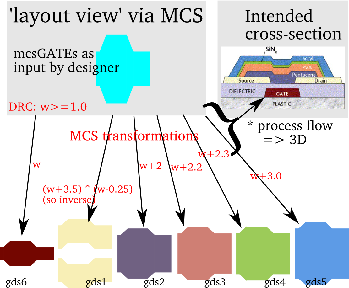
Instead of writing in many GDS layers, you can simply use the
xsection which represents
OptoDesigner's mcs concept which is shown in the picture.xsection
This defines axsection which in EDA-design is often called a cad or design layer.
In OptoDesigner this is a mcs. The xsection's define what the port should refer
to. A xsection is normally something like a waveguide or metal track and is often using
multiple (gds) layers. Very basic definition.
This definition is good for marking things up, but elements placed in this design layer will not go to a mask file.Including GDS mapping and some properties
MRL
Type pdaMRL documentation: Manufacturing Readiness Level (MRL) as defined by the EU.TRL
Type pdaTRL documentation: Technology Readiness Level (TRL) as defined by the EU.attribute
Type pdaAttributeType documentation: and views with information that is likely to be software specific. So it is more a 'flag' then a value. The value is just a string and not something with an expression in it.doc
Type pdaDocumentation documentation:This field allows some (short, few lines) documentation to be written. It can be a long string, but the idea is not to replace a design manual.
This fields is like
tex
which allows documentation in LaTex format; doc
is restricted to plain text.global
Type pdaNamedValue documentation:groupRef
Type pdaIdentifier documentation:Identifiers are used in the Python library for the
getName() and
setName() function and can thus be used to identify the different elements in list
s.In text the specification is a letter, followed by letters, numbers, underscore. The XSD schema validation is a regular expression: [A-Za-z]([A-Za-z0-9_])*
license
Type pdaLicense documentation:State the basic conditions of using the file and typically refer to legal documents.
License information should be compact enough to be clear as reference. The reference is expected to be to signed documents like Non Disclose Agreements (NDA) or service contracts and so on.
provider
Type pdaProvider documentation: provider, so a full company or institute name for example, instead of the smaller pdk_name.tapeout
other data file can be applied. Type pdaMPWrun documentation: library.tex
Type pdaTexDocumentation documentation:doc
, but tex can be a long text in LaTex format to
document the layer in more detail if needed.You can document anything relevant for the topic you want to define.
Multiple paragraphs is fine. Format is Latex, so more complex content is possible.