xPDK Layout
This section in a xPDK extends from xPDK_Header, so we will only describe the fields that are added with respect to the normal header.The layout section contains information for mask layout purposes as well as performing derived layer operations and (geometrical) design rule checking. It is therefore the key information for getting correct GDS files to a foundry.
The schema file can be downloaded or viewed: xPDK_Layout. It needs the xPDK_Base also, which is referenced via the http-link in the file.
The basic setup is to use
xsection's to draw your design in, as often waveguides need multiple GDS layers - for example a typical core, cladding and trench or some under/over etch compensation. This approach is not only suitable for photonics, but is practical in many technologies. The picture below shows a cross-section of a (printed) transistor.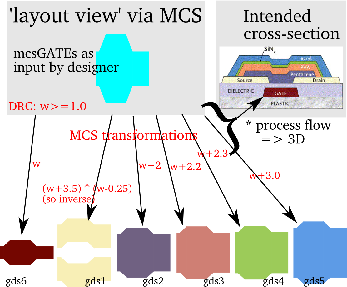
Instead of writing in many GDS layers, you can simply use the
xsection which represents OptoDesigner's mcs concept which is shown in the picture.Full example
The following example is a big one.xPDK_Layout.xml
Use:
xmllint --format -noout --schema xPDK_Layout.xsd xPDK_Layout.xml