pdaXsection
properties.Design layers which map via gridding onto GDS/Oasis/OpenAccess layers. xsection's provide for "optical" logic like default width, bend radius, coupling length and so on.
Each design layer can map to multipe GDS layers, so you can define a layer stack relating to a waveguide in a single definition.
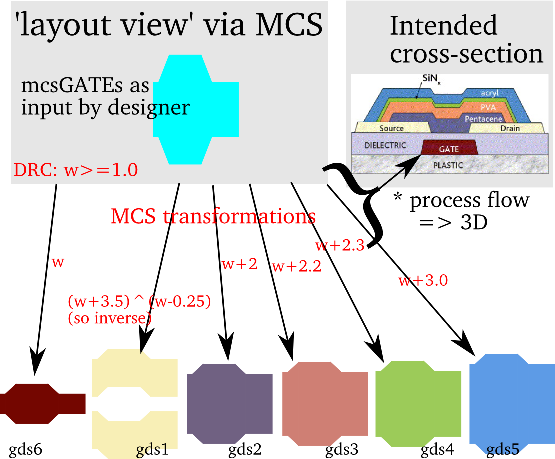
Take for example a typical core, cladding and trench or some under/over etch compensation. This approach is not only suitable for photonics, but is practical in many technologies. The picture below shows a cross-section of a (printed) transistor.
Instead of writing in many GDS layers, you can simply use the
xsection which represents
OptoDesigner's mcs concept which is shown in the picture.xsection
This defines axsection which in EDA-design is often called a cad or design layer.
In OptoDesigner this is a mcs. The xsection's define what the port should refer
to. A xsection is normally something like a waveguide or metal track and is often using
multiple (gds) layers. Very basic definition.
 <xsection name="WGbase">
  <purpose>Base waveguide</purpose>
 </xsection>
Including GDS mapping and some properties
<!-- define GDS layers for the <map> sections -->
<layer name="layer1">
 <gds_number>1</gds_number> <gds_datatype>0</gds_datatype>
</layer>

<layer name="layer2">
 <gds_number>2</gds_number> <gds_datatype>0</gds_datatype>
</layer>

<!-- define MCS layers -->
<xsection name="WG">
  <purpose type="active">Waveguide with grid</purpose>
  <grid>
   <map accuracy="0.1">layer1</map>
   <map widen="2">layer2</map>
  </grid>
  <xsSetWidth useDrc="false">0.5</xsSetWidth>
  <xsSetRadius min="100">200</xsSetRadius>
 </xsection>

 <xsection name="Doc">
  <purpose type="doc">Metal highlighting</purpose>
  <grid>
   <map accuracy="0.1">layer2</map>
   <map widen="2">layer2</map>
  </grid>
  <xsSetWidth useDrc="false">0.5</xsSetWidth>
  <xsSetRadius min="100">200</xsSetRadius>
 </xsection>
Structure
The attributes and elements are shown below, in a sorted per type fashion.In case a list is printed after an element, it indicates that you can have many, otherwise it should be a single element. With a optional it tells the element is not required.
<xsection maskNumber="..." mcsAnnotateBoundary="..." mcsAnnotateCellName="..." mcsAnnotateParameter="..." mcsAnnotatePinDC="..." mcsAnnotatePinInfo="..." mcsAnnotatePinOptical="..." mcsAnnotatePinRF="..." mcsAnnotatePinSize="..." mcsAnnotateText="..." mcsAnnotateWaveguide="..." mcsBusConfig="..." mcsMigrate="..." name="..." pdkSelect="..." techLayerID="..." techLayerRouting="..." xstype="..." ... > ...
<DesignRule> ... </DesignRule> list
<MRL> ... </MRL> list
<TRL> ... </TRL> list
<WaiveReport> ... </WaiveReport> list
<color> ... </color> list
<doc> ... </doc> list
<fillstyle> ... </fillstyle> list optional
<grid> ... </grid> list
<groupRef> ... </groupRef> list
<linestyle> ... </linestyle> list
<module> ... </module> list
<purpose> ... </purpose> list
<sptFooter> ... </sptFooter> list
<sptHeader> ... </sptHeader> list
<techLayerConnection> ... </techLayerConnection> list
<tex> ... </tex> list
<ticket> ... </ticket> list
<visible> ... </visible> list
<wavelength> ... </wavelength> list
<xsSetGap> ... </xsSetGap> list
<xsSetPortCriticalRadius> ... </xsSetPortCriticalRadius> list
<xsSetRadius> ... </xsSetRadius> list
<xsSetSBOffset> ... </xsSetSBOffset> list
<xsSetTaperAngle> ... </xsSetTaperAngle> list
<xsSetTextExpand> ... </xsSetTextExpand> list
<xsSetUncoupledDistance> ... </xsSetUncoupledDistance> list
<xsSetWidth> ... </xsSetWidth> list
</xsection>
XSD The schema file can be downloaded or viewed at xPDK_Base.
Details
DesignRule
Define a 'meta rule', so non-geometric. Type pdaDrcGeneralRule documentation: Define a design rule that is not layer or "polygon" / "geometric" based.Design rules are available in different flavors, some of which can not be associated with layers; for example the name of the GDS cell that is required to be used for the design.
The rule is described in text and software may (or not) be able to implement them. Using the rule field gives designers an easy way to find more information on the DRC fail if it appears.
MRL
Type pdaMRL documentation: Manufacturing Readiness Level (MRL) as defined by the EU.TRL
Type pdaTRL documentation: Technology Readiness Level (TRL) as defined by the EU.WaiveReport
Type WaiveReport documentation: Waive an issue in the Report.htmlcolor
this is intended to have more consistent look over different software. Type pdaColor documentation: Each of R, G and B is required and be between 0 and 256.doc
Type pdaDocumentation documentation:This field allows some (short, few lines) documentation to be written. It can be a long string, but the idea is not to replace a design manual.
This fields is like
tex
which allows documentation in LaTex format; doc
is restricted to plain text.extend
Type AllowExtend documentation: Allows to extend with any (complex) data for enriching a design kit. The sub-data of an
extend will normally be vendor or provider specific, but may span multiple software
vendors or suppliers.Provider extensions can be references to (or embedded) reporting scripts or their versions; source database references and so on. Such data is helpful in cross-referencing production issues or differences between export snapshots. Embedding such data in the XML rather then side-files enhances tracebility and reduces errors.
Using this section is not considered part of the xPDK format therefore, but as long as the files validate with the Stichting PDAFlow Foundation schema's, it is not considered a (not allowed) Derivative version.
For conventions, please check also Extensions.
See also xPDK License.
fillstyle
(polygon area) default settings in software; this is intended to have more consistent look over different software.Type pdaFillStyle documentation:
FILLfilled - used in OptoDesignerNOFILLnot filled - used in OptoDesignerSOLIDSolid style.DOTDotted style.LONG_DASHLong dashed style.SHORT_DASHShort dashed style.DOT_DASHDot and dash style.TRANSPARENTnot filled - used in OptoDesigner.STIPPLEUse the stipple style.BDIAGONAL_HATCHBackward diagonal hatch.CROSSDIAG_HATCHCross-diagonal hatch.FDIAGONAL_HATCHForward diagonal hatch.CROSS_HATCHCross hatch.HORIZONTAL_HATCHHorizontal hatch.VERTICAL_HATCHVertical hatch.
grid
gdslayer is a key aspect. It is handled in thegrid section where
many maps can be defined.Each mapping adds a possibly modified copy using the widening or lengthening of the data to the respective gdslayer.
You can define a mix of
widen, lengthen, accuracy
and so on per map and they will be jointly used for one mapping to the GDS
layer in the <map>...</map>. The name in<map>...</map> should be
the name of a layer or applayer.The examples show only a single attribute per map to keep the example more focussed and the documentation more specific.
An
xsection can have zero grids, this makes it a
display-only layer. To get something into GDS/Oasis/OpenAccess you need to have one or
more gds-layers associated. Each can have a different widening.
Type pdaXsectionGridToLayer documentation:
groupRef
Type pdaIdentifier documentation:Identifiers are used in the Python library for the
getName() and
setName() function and can thus be used to identify the different elements in list
s.In text the specification is a letter, followed by letters, numbers, underscore. The XSD schema validation is a regular expression: [A-Za-z]([A-Za-z0-9_])*
linestyle
contour) default settings in software; this is intended to have more consistent look over different software.Type pdaIdentifier documentation:
Identifiers are used in the Python library for the
getName() and
setName() function and can thus be used to identify the different elements in list
s.In text the specification is a letter, followed by letters, numbers, underscore. The XSD schema validation is a regular expression: [A-Za-z]([A-Za-z0-9_])*
maskNumber
Type maskNumber documentation: Define tech maskNumber.This number somewhat reflects the layerstack and is used in LVS. The lower numbers should be the lower layers in the chip. The range does not need to be continous.
mcsAnnotateBoundary
Type mcsAnnotateBoundary documentation: OptoDesigner extension, use this xsection/mcs for the BB/pcell name in xpdkAnnotator().mcsAnnotateCellName
Type mcsAnnotateCellName documentation: OptoDesigner extension, use this MCS for the BB/pcell name in xpdkAnnotator().mcsAnnotateParameter
Type mcsAnnotateParameter documentation: OptoDesigner extension, use this MCS for BB/pcell parameters in xpdkAnnotator().mcsAnnotatePinDC
Type mcsAnnotatePinDC documentation: Tag DC port in this layer via rectangle.mcsAnnotatePinInfo
Type mcsAnnotatePinInfo documentation: OptoDesigner extension, use this MCS for BB/pcell ports in xpdkAnnotator(). This layer is used for the port name and properties.mcsAnnotatePinOptical
Type mcsAnnotatePinOptical documentation: Tag optical port in this layer via rectangle.mcsAnnotatePinRF
Type mcsAnnotatePinRF documentation: Tag RF port in this layer via rectangle.mcsAnnotatePinSize
Type mcsAnnotatePinSize documentation: OptoDesigner extension, use this MCS for BB/pcell ports in xpdkAnnotator(). This layer is used for a rectangle that indicates the width of the port.mcsAnnotateText
Type mcsAnnotateText documentation: Extension, use this MCS for plain text.mcsAnnotateWaveguide
Type mcsAnnotateWaveguide documentation: This information is intended for Layout-vs-Schematic (LVS) with ICvalidator in OptoCompiler.mcsBusConfig
Type mcsBusConfig documentation: This boolean can be set to true to set up a curve-based bus-config for this xsection in case no BBs are set up for bus-routing for this xsection.Using this value is not needed if there is at least a single BB configured for being a busConfig-element for this xsection; in that case the other non-specified layout's are automatically configured using basic OptoDesigner curves.
mcsMigrate
Type mcsMigrate documentation: and thus to slowly be dropped from the design kit.module
Type pdaIdentifier documentation:Identifiers are used in the Python library for the
getName() and
setName() function and can thus be used to identify the different elements in list
s.In text the specification is a letter, followed by letters, numbers, underscore. The XSD schema validation is a regular expression: [A-Za-z]([A-Za-z0-9_])*
name
Type pdaIdentifier documentation:Identifiers are used in the Python library for the
getName() and
setName() function and can thus be used to identify the different elements in list
s.In text the specification is a letter, followed by letters, numbers, underscore. The XSD schema validation is a regular expression: [A-Za-z]([A-Za-z0-9_])*
pdkSelect
Type pdkSelect documentation: Use in layout.xml's to have a single foundry database, where you select layer/xsection/.. sub-sets for a given PDK.purpose
this is a short line. Type pdaLayerPurpose documentation: An optional attribute is type which can have one of the following values: passive, active, doc, misc, metal, metalalt, metalrouting, metal1, metal2, metal3, metal4, metal5, metal6, metal7, metal8, metal9, rf, rf_gsg, rf_gssg, rf_s, rf_g.Metal1-9 are for multi-layer metal, with '1' being closes to the photonics; moving up to higher numbers is typically done with VIA's.
sptFooter
Type sptFooter documentation: This section will be put at the end of a definition via XSLT.Tech/02 definition
This section is copied into the '02' file just before the function export()The typical use is for backward compatability (for example mapping older mcs names) or some custom tech functions that need access to most of the tech-file.
Using this element instead of the TechFooter is easier in case of enriching the design kit via the C++ or Python library.
pdaSingleLayerOPS
This section is copied into the '02' file below the (gds/mcs) layer definitions in the single-layer operation block. It is intended for more complex single/multi layer derived operations or DRC.Download the xsl/xml/xsd's and run the (bash) command line below to convert the XML to a SPT example in OptoDesigner (see short docu):
xsltproc --xinclude -stringparam standalone true -stringparam example drc0 xPDK_toOptoDesigner02.xsl layer_singleSpt.xmlfull file
    <gds_datatype>0</gds_datatype>
    <grid>0.001</grid>
    <purpose>Waveguide layer</purpose>
    <color R="100" G="200" B="255"/>
    <visible>true</visible>
    <fillstyle>NOFILL</fillstyle>
    <linestyle>fill</linestyle>
  </layer>
  <layer name="layer2">
    <gds_number>2</gds_number>
    <gds_datatype>0</gds_datatype>
    <grid>0.001</grid>
    <purpose>Waveguide layer</purpose>
    <color R="255" G="20" B="20"/>
    <visible>true</visible>
    <fillstyle>NOFILL</fillstyle>
    <linestyle>fill</linestyle>
    <od:sptFooter>
      // println("hi");
   </od:sptFooter>
  </layer>
Spt:
xsection
This section is copied into the '02' file below the mcs definition and is intended for more complex properties like waveguide models and so on.It provides also for less common mcsSet*() functions or feeding them with values that xPDK does not support.
 </doc>

 <xsection name="WG">
  <od:sptHeader>// This section does some special OptoDesigner things.
   mcsSetCurveCheck();
   mcsSetAltWG("WGhigh","WGlow");
  </od:sptHeader>
 </xsection>
BB definition
This section is copied into the '04' file inside the layout definition and is intended for fine-tuning behavior, giving control over returned attributes and so on. In typical cases it is not needed.Use this field in case the xPDK format does not have all the fields you need for your BB in OptoDesigner. For example this is possible for returning more layout attributes or supporting more complex design rule checking.
<bb name="myBB">
 <port label="in0">
  <position>
     <x>0</x>
  </position>
 </port>
 <od:sptFooter>
  ml::Straight(cin-> this@in0:wfix(1),20) elm;
  this{"elm"}=elm;
  this{"L"}=20;
 </od:sptFooter>
</bb>
BB boundary
This section is copied into the '04' file into the layout itself and can be used to mark up complex boundaries. Also the use of multiple mcs/gds layers for DRC can be simpler this way.Instead of using spt, you can also use the xsection for typical cases and reduce vendor dependence for this section.
 </doc>

<bb name="myBB">
 <port label="in0">
  <position>
     <x>0</x>
   </position>
 </port>
 <boundary>
  <od:sptHeader>
   ml::Straight(cin-> this@in0 : wopar(1,3),20);
  </od:sptHeader>
 </boundary>
</bb>
sptHeader
Type sptHeader documentation: This section will be put at the start of a definition via XSLT.Tech/02 definition
This section is copied into the '02' file at the start of the TechnologyPDKLIB class instance.The typical use is waveguide mode models and other bigger spt sections that can then be used in the different sections.
pdaSingleLayerOPS
This section is copied into the '02' file below the (gds/mcs) layer definitions in the single-layer operation block. It is intended for more complex single/multi layer derived operations or DRC.Download the xsl/xml/xsd's and run the (bash) command line below to convert the XML to a SPT example in OptoDesigner (see short docu):
xsltproc --xinclude -stringparam standalone true -stringparam example drc0 xPDK_toOptoDesigner02.xsl layer_singleSpt.xmlfull file
    <gds_datatype>0</gds_datatype>
    <grid>0.001</grid>
    <purpose>Waveguide layer</purpose>
    <color R="100" G="200" B="255"/>
    <visible>true</visible>
    <fillstyle>NOFILL</fillstyle>
    <linestyle>fill</linestyle>
  </layer>
  <layer name="layer2">
    <gds_number>2</gds_number>
    <gds_datatype>0</gds_datatype>
    <grid>0.001</grid>
    <purpose>Waveguide layer</purpose>
    <color R="255" G="20" B="20"/>
    <visible>true</visible>
    <fillstyle>NOFILL</fillstyle>
    <linestyle>fill</linestyle>
    <od:sptFooter>
      // println("hi");
   </od:sptFooter>
  </layer>
Spt:
xsection
This section is copied into the '02' file below the mcs definition and is intended for more complex properties like waveguide models and so on.It provides also for less common mcsSet*() functions or feeding them with values that xPDK does not support.
 </doc>

 <xsection name="WG">
  <od:sptHeader>// This section does some special OptoDesigner things.
   mcsSetCurveCheck();
   mcsSetAltWG("WGhigh","WGlow");
  </od:sptHeader>
 </xsection>
BB definition
This section is copied into the '04' file inside the layout definition and is intended for fine-tuning behavior, giving control over returned attributes and so on. In typical cases it is not needed.Use this field in case the xPDK format does not have all the fields you need for your BB in OptoDesigner. For example this is possible for returning more layout attributes or supporting more complex design rule checking.
<bb name="myBB">
 <port label="in0">
  <position>
     <x>0</x>
  </position>
 </port>
 <od:sptFooter>
  ml::Straight(cin-> this@in0:wfix(1),20) elm;
  this{"elm"}=elm;
  this{"L"}=20;
 </od:sptFooter>
</bb>
BB boundary
This section is copied into the '04' file into the layout itself and can be used to mark up complex boundaries. Also the use of multiple mcs/gds layers for DRC can be simpler this way.Instead of using spt, you can also use the xsection for typical cases and reduce vendor dependence for this section.
 </doc>

<bb name="myBB">
 <port label="in0">
  <position>
     <x>0</x>
   </position>
 </port>
 <boundary>
  <od:sptHeader>
   ml::Straight(cin-> this@in0 : wopar(1,3),20);
  </od:sptHeader>
 </boundary>
</bb>
techLayerConnection
Type techLayerConnection documentation: Define OA-Tech layer connection.This field can be used to link layers and/or xsections; this tells that routing-wise ('design intent') they are directly connecting, possibly with a byLayer value.
You can define the connection in either layer/xsection, no need to define it twice.
For layer/xsection's that connect to more than one, define them from one layer, otherwise multiple lines will be written in the tech file.
Only use this for layers that have at least one of techLayerRouting='true' or techIncludeElectricalTag='true'.
techLayerID
Type techLayerID documentation: Define OA-Tech ID.The OA Tech file needs to have unique numbers that are PDK version constant for design migration. The default behavior is use to use for layer definitions 65536*gds_number+gds_datatype and for the xsection the value 10000+N with N being the index in the xsection list.
Those values are very likely to be unique per PDK, but the xsection numbers are unlikely to be PDK version constant (adding or removing xsection's will fail this).
You can overrule the Tech ID with this field; the range is 256-10000 to avoid overlapping the default range. The number is free within this range, but as guideline:
- 1000 - 1999 use this range for optical layers
- 2000 - 2999 use this range for electrical layers
- 3000 - 3999 use this range for mask annotations
- 4000 - 4999 use this range for LVS recognition
techLayerRouting
Type techLayerRouting documentation: Mark for routing in in OptoCompiler tech file, section 'constraintGroups'tex
Type pdaTexDocumentation documentation:doc
, but tex can be a long text in LaTex format to
document the layer in more detail if needed.You can document anything relevant for the topic you want to define.
Multiple paragraphs is fine. Format is Latex, so more complex content is possible.
ticket
Type pdaTicket documentation:visible
intended to have more consistent look over different software.wavelength
Type wavelength documentation: For the xsSet--() functions the wavelength is important; the xPDK standard assumes single-band definitions for now, but multi-band / wavelength support is needed. This field is therefore likely to move towards the standard.The options in this field are used for wavelength / band selection in the technology. The field itself is a string, so you can use things like "C" or "O-band" as well as values like "0.2 um" or "1550 nm".
xsSetGap
uncoupled. It relates to mcsSetUncoupledDistance, but this is suitable for tapering elements also.
 <xsection name="WG">
  <xsSetGap>2.0</xsSetGap>
 </xsection>
xsSetPortCriticalRadius
"straight".Using this is typically for a low contast waveguides which need SBoffsets. Radii above this value are ignored in connectivity tests to avoid radius conflicts where unneeded. With radius below this value, the design software can give warnings on mismatch in radius, which indicates you need transition elements (in schematic design) or (in layout-only design) a geometrical offset to ensure low transistion losses in the guided modes.
You can use a negative value to disable those tests. The test should only be done in case the port-radius is set, so not using them will also block such connections warnings. Type pdaExpressionXt documentation:
xsSetRadius
curved / bended waveguides.The waveguide/port bend radius is measured with respect to the geometrical waveguide center (in the case of most common symmetric waveguides).
Using this value in the BB-sections of xPDK simplifies maintenance. It also shows better the intent of certain equations / values.
 <xsection name="WG">
    <xsSetRadius useDrc="false" min="1">50.0</xsSetRadius>
 </xsection>
If min is set, then OptoDesigner will also validate curves against this value - so the "logical" value rather (per-se) the geometrical value as due to grid/map you may have different values for that.
If this is not intended, use useDrc="false" as attribute.
xsSetSBOffset
transistion for the default width/radius.You can use the <spt> to define more complex (radius dependent) values also or apply a complete mcsModeModel for that.
These are OptoDesigner specific values, but the typical width/radius is often used.
 <xsection name="WG">
  <xsSetSBOffset>0.01</xsSetSBOffset>
 </xsection>
xsSetTaperAngle
for automatic tapers when width-changes are detected.Recommended is to use an angle that is low enough to avoid mode or polarisation conversion.
 <xsection name="WGbase">
  <xsSetTaperAngle>1.0</xsSetTaperAngle>
 </xsection>
xsSetTextExpand
grow the pixels of a text font.This is often needed to prevent design rule fails on small vertices or sharp angles.
 <xsection name="WG">
  <xsSetTextExpand>20</xsSetTextExpand>
 </xsection>
xsSetUncoupledDistance
curves for which they are to be reasonably uncoupled.The reasonable is not a hard specification, but indicative. Reasonable values are when the coupling length will be close to the chip length.
 <xsection name="WG">
  <xsSetUncoupledDistance>2.0</xsSetUncoupledDistance>
 </xsection>
xsSetWidth
Using this value in the BB-sections of xPDK simplifies maintenance. It also shows better the intent of certain equations / values.
 <xsection name="WG">
  <xsSetWidth useDrc="false" min="0.1">0.5</xsSetWidth>
 </xsection>
If min is set, then OptoDesigner will also validate curves against this value - so the "logical" value rather (per-se) the geometrical value as due to grid/map you may have different values for that.
If this is not intended, use useDrc="false" as attribute.